Samsung Reveals Next Generation NAND Technology That Cuts Power Use by 96 Percent
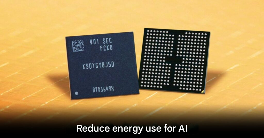
Samsung is once again reinforcing its position as a global leader in memory innovation with a breakthrough that is turning heads across the tech industry. Recent reports highlight that the company is preparing to showcase its LPDDR6 technology at CES next year, but what truly captured attention is the dramatic leap in NAND flash efficiency. This next generation NAND solution reportedly reduces power consumption by up to 96 percent, a figure that immediately impacts how AI data centers, smartphones and high-performance computing devices may evolve in the near future as demand for energy efficiency continues to surge.
This advancement is not speculation but is backed by research published in the prestigious journal Nature under the title “Ferroelectric Transistor for Low-Power NAND Flash Memory.” The study comes from a 34 member research team that investigated oxide semiconductor technology. While oxide semiconductors are not traditionally favored for high performance processors due to their high threshold voltage, the team found unique advantages that could transform how NAND flash memory is designed.
The core principle behind this new technology lies in using oxide semiconductor properties to block subthreshold currents more effectively. This lowers leakage significantly and improves power control across NAND structures. As NAND chips adopt increasingly stacked architectures with longer cell chains, leakage becomes more prominent and energy requirements escalate. Addressing this issue is essential as modern systems continue to demand more storage and faster access than ever before.
The research team introduced a new mechanism specifically created to reduce energy losses that occur during read and write operations in multilayer NAND designs. Their findings indicate a power reduction of up to 96 percent when compared with traditional NAND chips, marking a massive milestone for the industry. This positions the technology as an important piece of the puzzle for future data heavy infrastructure and devices, particularly in an era defined by rapid AI expansion.
Although Samsung has not yet given a timeline for when this power efficient NAND technology will enter mass production, its potential impact is already sparking anticipation. Once it becomes commercially available, the benefits are expected to spread across the entire memory ecosystem. Data center operators handling intensive AI workloads could significantly reduce operational power demands, and smartphone manufacturers might finally unlock new levels of battery efficiency without sacrificing performance.
For now, the industry is watching closely as this breakthrough moves toward practical deployment. Its journey will likely coincide with the arrival of new storage standards such as UFS 5.0, which is expected to transform future mobile devices. All eyes are on Samsung as the company works to bring this long awaited innovation from the lab to real world applications in a smooth and scalable way.